DenciTec®
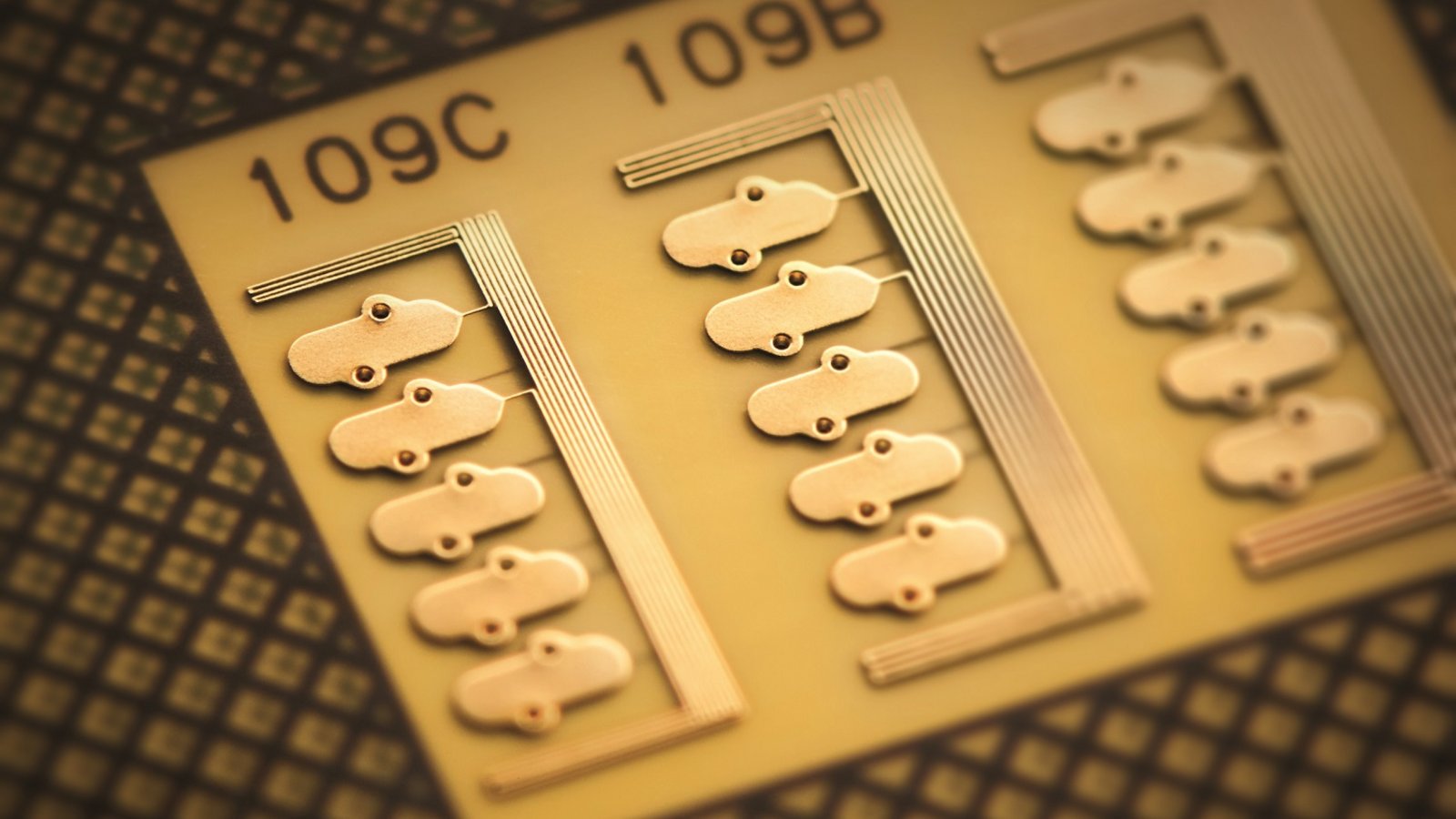
Since 2016 Cicor has been offering DenciTec® PCBs. Highly sophisticated manufacturing technologies are enabling the production of very high-density circuits. State of the art equipments and new kinds of base-materials are making sure, that no concessions have to be made for Qality and design freedom..
DenciTec® makes further miniaturization possible:
Line widths and spacings down to 25 µm (1 mil)
Copper thicknesses of 20 µm (0.8 mil) +/- 5 µm on all layers
Laser-via diameters of 30 µm (1.4 mil)
Annular rings of 30 µm (1.2 mil) for the inner layers and 20 µm (0.8 mil) for the outer layers
Copper-filled blind vias with the option of via stacking and vias-in-pads
Even ultra-thin circuits are possible, using a 12.5 µm (0.5 mil) polyimide core material (4-layer flex circuits less than 120 µm (4.7 mil) thick)
Maximum reliability
More freedom in design – greater functionality for equipment:
Miniaturization: Significantly greater integration capabilities: More space for additional options such as energy supply (batteries, etc.)
Higher packing density: More design options, no limitations in the use of design features
Greater functionality: Smarter products with more functions
Significantly lower manufacturing costs than with thin-film technology
PCB site
We are here for you
Our PCB team is available to answer any questions about Cicor and our solutions.